Dc-Dc Converter Trends and Output Filter Cap Requirements
John Maxwell, Director of Product Development - March 1, 2006Introduction
Historically the volume Dc-Dc converter market has been driven by telecommunications equipment powered by 48V isolated "Brick" DC/DC converters. Technologies used today in the design and manufacture of different high density custom semiconductors or ASIC (Application Specific Integrated Circuit) has resulted in a proliferation of power supply voltages and increased supply or load current requirements for these semiconductors. Today numerous different voltages can be encountered in systems each with different load currents and power on or sequencing requirements precluding multiple Brick converters. New power systems use a limited number of isolated bricks and a number of POL (Point Of Load) converters.
ASIC voltage requirements are dropping resulting in dramatically reduced margins for ripple, noise, load variations and voltage drop in power planes within the system board. These voltage drops have evolved power system architectures to minimize the effect of these drops voltage drops within power distribution planes. Current total noise, ripple, DC voltage drift and voltage drop within power planes are fast approaching +/- 1% of the converter output voltage or +/- 15mV for a 1.5V output voltage.
Small physical size, minimum parasitic values and high capacitance have become mandatory for these small POL converters.
Examples of Power Plane Voltage Drop
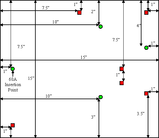
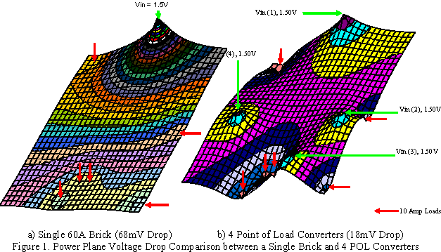
Copper plane thickness of ½ oz (0.7 mil) is typically used in many 20+ layer boards in telecommunications systems. There are boards that use 1 oz layer copper thickness and some even use 2 oz copper layers for ground and power planes. Results are only presented for room temperature but copper has a temperature coefficient of +0.393% / ° and can significantly increase voltage drops in both voltage and ground planes used in these large boards. A 50° board temperature rise increases copper resistivity and corresponding power plane voltage drops by nearly 20%. Appendix 1 lists the location of each voltage injection point and current sink or load on a 15" (38cm × 38cm) square telecom board. Both a single "Brick" and distributed POL power scheme were analyzed to compare DC voltage drops across a ½ oz single power plane with six 10A loads representing an ASIC at each location. Voltage drops will be the same for the ground plane. Load and source locations are listed in the appendix.
These two cases are simulated using finite difference techniques that take into account copper thickness and temperature coefficients. In the first case a single 60A brick provides all of the current for the board. The second case uses four POL (Point of Load) DC/DC converters to supply the single power plane with current. The location for those POL converters was chosen to minimize power plane voltage drops. Voltage drops on the ground plane will be a mirror image of the power plane doubling the total voltage drop at any load point. Voltage gradients have shown (color changes) for each simulation represents a 2 mV difference.
Output Filter Capacitors
Ripple current in a buck converter switching at 500 kHz will be used and is shown in Figure 2. The first parameter to be considered will be maximum output loop inductance and capacitor ESL as it has been traditionally ignored in the past but becomes critical as the physical size of converters shrink. We cannot look to the past when output filters were carpet bombed with capacitors but designers must now understand what the minimum/maximum limits of ESL, ESR and capacitance are.
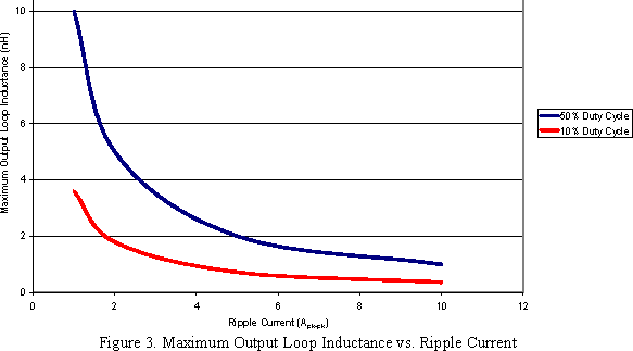
Maximum Output Filter Loop InductanceThis is not just the inductance of the capacitor (ESL) but must include interconnect inductance in the output loop of the converter filter. Trace width and length now become part of the calculus of output filters.
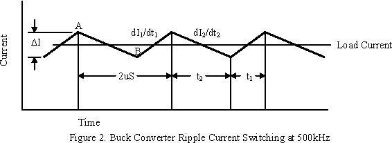
The largest di/dt is at current inflection points where current is sourced from different portions of the circuit. The voltage across an inductor V = L di/dt or L = ΔV(dt/di). Knowing the total allowed ripple voltage (+/- 10mV) a plot of absolute maximum output loop inductance vs. ripple current. For example the inductive at point A will be negative and positive at point B. This plot would assume no contributions due to loop resistance or capacitance. The total current change at point A and B is the sum of the slopes or dI1/dt1 + dI2/dt2. Converter input and output voltage and load current determine the duty cycle which impacts maximum output loop inductance and capacitor ESL. Few converters will operate near 50% duty cycle but will typically operate in the 10-20% range severely limiting the total output loop inductance and corresponding capacitor ESL.
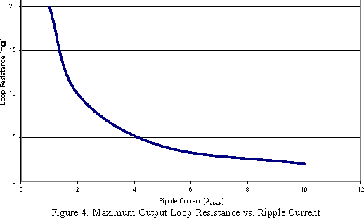
Maximum Output Filter Loop Resistance
Like in the loop inductance calculations now the total contribution of output ripple and noise will be determined assuming no contribution from either the inductance or capacitance. Again 20mV will be used for ΔV = ΔI × R(Loop Resistance) or R = ΔV/ΔI.
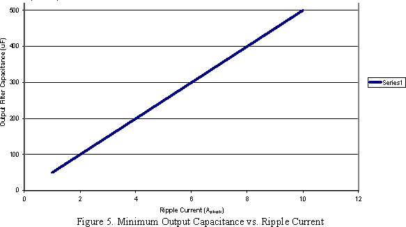
Minimum Output Filter Capacitance
As in the two previous examples calculations will be based on the total contribution of ripple and noise by the output filter capacitance only. The basic capacitor equation of I = C dV/dt or C = ΔI × (dt/ΔV).
The three critical minimum and maximum lumped parameters (inductance, resistance and capacitance) have been analyzed for the common buck converter topology used in POL Dc-Dc converters. Increases in switching frequencies, shorter inductor conduction time and increased load currents all impact output filter characteristics. Increases in frequency decrease output filter capacitance required to control ripple voltage but increases switching noise due to output filter inductance. The one parameter that is basically frequency independent is filter loop resistance while output capacitance has a marked impact on output ripple and noise.
Output Capacitor Filter Technologies
There are three main competing capacitor technologies for output filter applications. Multi-layer ceramic, tantalum/niobium oxide and polymer aluminum electrolytic capacitors are all used in Dc- Dc output filters. Small size and high performance of POL converters drive the choice of output filter capacitors. Inductance is the primary driver because not only does the capacitor ESL need to be low but it is further limited on board trace and interconnect inductance.
High current/low resistance and inductance require large broad interconnects between the POL and board that it is mounted to. The shift to lead free solders further complicates the design due to the brittle nature of lead free solders driving interconnect dimensions for solder joint reliability but increasing both inductance and resistance.
Capacitor choices need to be evaluated first based on inductance, then ESR and finally total capacitance required. Basically all technologies meet the maximum loop resistance so the focus is on inductance. Table 1 is a list a typical ESL, ESR and capacitance values for different capacitor technologies and allows the designer to choose what will work as output filter capacitors for each design.
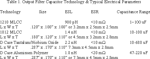
MLCC or multi-layer ceramic capacitors have the clear edge in size, lead free process compatibility and inductance. Tantalum and polymer aluminum capacitors have the edge in capacitance but that gap is shrinking as dielectric layer thickness is reduced in ceramic capacitors. Converter size is shrinking and switching frequencies are increasing reducing filter capacitance and maximum inductance. These requirements preclude the use of the larger case size of tantalum/niobium oxide and polymer aluminum capacitors from many Dc-Dc converter applications.
Appendix
Locations of Voltage Injection Points and Loads on Test Board for Power Plane Voltage Drop Simulation.