Capacitor Cracks: Still with Us After All These Years
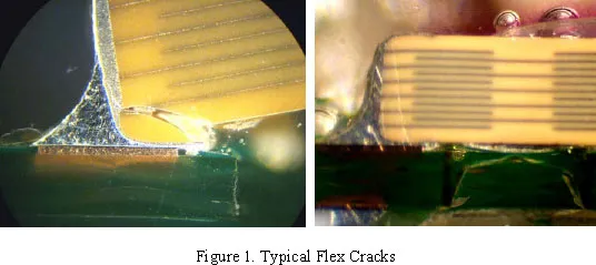
Cracked SMT capacitors and their root causes have been discussed at length in the literature1,2,3,4,5 for years. Cracked capacitors can manifest themselves as latent defects such as increased leakage current, intermittent opens or shorts or no problem found when field returned assemblies are analyzed. In some cases those defects can lead to catastrophic failure depending on the application and energy available. Cracks could be introduced at virtually any point in the surface mount assembly process from pick and place, soldering and assembly handling after soldering. Understanding the application, assembly process and final product configuration are necessary to eliminate capacitor cracking.
Things have changed to change the face of capacitor cracking during the past two decades. Improved pick and place equipment have virtually eliminated that source of cracking as the equipment designers took capacitor cracking seriously and eliminated it as a source. Manufacturers and users of wave soldering equipment now better understand sources of thermal shock and most wave solder machines have adequate preheat control and have minimized that source of cracking except on big chips like 1812 (4.5 x 2.5mm) and larger or thick chips (>0.050" or 1.25mm) of any case size. But what are still with us after all these years is board flexure cracking during handling, test and assembly after soldering. Industry standards groups and manufacturers now have flex specifications for ceramic capacitors but on board flexure or bending often can exceed the capability of those capacitors.
Board Flexure and Standard Testing
Today as well in the past board flexure is the largest source of capacitor cracking and designers must understand how PWB (Printed Wiring Board) layout impacts assembly and reliability. Ceramic capacitors need to be isolated away from flexure zones such as board corners and edges, connectors, large mass components like inductors/transformers and mounting holes.
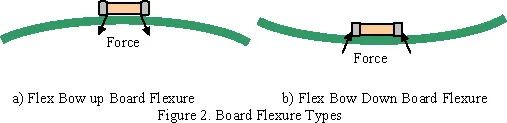
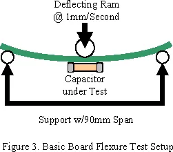
Bow up flexure is the configuration used in evaluating ceramic capacitor termination to body performance under JIS-C-6429 and CECC32100. Under those test standards an evaluation board 1.6mm thick is supported in a 90mm span, the capacitor is reflow soldered to pads on the board in the board center parallel to the long axis. A ram presses on the back side of the board with a speed of 1mm/second. Defects are detected using continuous capacitance monitoring and detecting capacitance drop during flexure. Fixtures for bow down flex conditions are very difficult to perform because the deflecting ram must surround the part on all sides. Additionally there would be discontinuities at localized zones on the PWB around the chip termination.
Current flexure standards specifications are > 1mm under these test conditions. There are things that can be done during board layout to minimize flexure cracking and additional actions that can be taken once a board is in production.
PWB (Printed Wiring Board) Layout Guidelines to Minimize Cracking
The following guidelines are to aid the board layout and circuit designer and manufacturing engineer in identifying areas where capacitor cracking is most likely to occur and where changes may be made to minimize this source of defects.
General Guidelines
- Do not mount ceramic capacitors perpendicular to board edges
- Avoid mounting along board edges or corners during layout
- Avoid mounting holes during layout
- V grove board separation is very stressful during board separation, avoid if possible, otherwise pre-route the board
- Perforated breakout tabs or mouse bites are stressful and isolate ceramic capacitors away from those areas
- Avoid board twisting
- Keep parts isolated from where the assembly is handled especially when inserted into test systems
- Never probe chip terminations, use separate test pads
- Analyze bending when assemblies are placed into production totes especially when slid into slots
- Analyze when the assembly is installed into final product
- Pay attention to natural flex or bend zones when the assembly is mounted
- Remove solder mask from between pads if no traces or PTH (Plated Thru Holes)
- Eliminates solder mask that can act as a fulcrum during board flex concentrating stress in capacitor corners
- Minimized trapped flux pulled between terminations by capillary forces during reflow and is especially important if water soluble flux is used or if high voltage is applied across the chip to minimize arcing
- Solder mask acts as a fulcrum during reflow soldering and if too thick can cause draw bridges and open solder joints in 0402 and 0603 chips
- Small assemblies are particularly troublesome due to all of the above
- Pay attention mounting ceramic capacitors around connectors
- Avoid using soldering irons especially now that the world is moving to lead free solders with corresponding higher soldering temperatures
Large Part Guidelines (>1210 Case Size)
- Avoid board edges during layout (>0.200" or 5mm)
- Never wave solder these parts
- Keep solder fillets small (See IPC-D-2796 and IPC-A-610D7)
- Do not force cool after soldering
- Watch where people put their fingers and thumbs while handling assemblies, big flat smooth capacitors are always preferred by operators
- Pad design is not a critical issue with large parts due to their mass holds them in place
- Do not mount near large heavy components (>0.200" or 5mm)
- Do not mount near connectors (>0.200" or 5mm)
- Never use soldering irons
Ceramic capacitor cracking will be with us for the foreseeable future but the impact on assemblies can be dramatically minimized by proper board layout and manufacturing of the assembly. These guidelines are provided to aid in eliminating cracked capacitors.
References
- Maxwell, J., "Cracks: The Hidden Defect," 28th Electronics Component Conference, 1988, pp. 376-384
- Maxwell, J., "Manufacturing Induced Defects" EXPO SMT International 89, September 25, 1989, pp.53-5
- Maxwell, J., "Zero Defect Design Check List For Surface Mount" CARTS, March 28, 1990, pp.40-50
- Maxwell, J., "Cracked Capacitors: Causes and Solutions", SURFACE MOUNT INTERNATIONAL, September 1996, Invited Paper for Open Sessions
- Maxwell, J., "Board Flexure Comparison Between Surface Mount Multi-Layer Ceramic and Film Capacitors", CARTS, March 1999, pp. 251-255
- IPC-D-279, "Design Guidelines for Reliable Surface Mount Technology Printed Board Assemblies," July 1996
- IPC-A-610D, "Acceptability of Electronic Assemblies," April 5, 2005
Notice: Specifications are subject to change without notice. Contact your nearest Johanson Dielectrics Sales Office for the latest specifications. All statements, information and data given herein are believed to be accurate and reliable, but are presented without guarantee, warranty, or responsibility of any kind, expressed or implied. Statements or suggestions concerning possible use of our products are made without representation or warranty that any such use is free of patent infringement and are not recommendations to infringe any patents. The user should not assume that all safety measures are indicated or that other measures may not be required. Specifications are typical and may not apply to all applications.