Pad Design & Spacing Impact on AC Breakdown
High voltage capacitors are used for isolation and transient protection in electronics thatare connected to either phone lines using modems or Ethernet connections. Portable electronics that use those components are driving to smaller case sizes to increase product functionality while shrinking both size and weight. As the users of high voltage capacitors continue driving to smaller high voltage (HV) components, understanding arcing failures becomes critical in designing and manufacturing those assemblies. There are interactions between the PWB (Printed Wiring Board) flux residues, humidity absorption of the board solder mask and flux residue, solder paste used, pad or land shape and spacing. These end product changes require optimum board layout to achieve both functionality and size/weight reductions.
The influence of solder mask beneath parts and slots between component pads have already evaluated(1) for 1206 and 1808 case sizes and that work was used as the springboard for this study. Observations of both bare boards used in high voltage arcing tests showed that the arcs were originating at component pad corners in the previous study.This was the driving force behind evaluating SMT pad shape and spacing impact on high voltage breakdown performance.
Experiment
This study uses two case sizes, 1206 and 1808 sized capacitors with radius vs. square corner pads using slightly different pad spacing to determine improved assembly performance when these capacitors are used. Bare boards and capacitors are tested to failure under AC breakdown conditions to establish a performance baseline. Capacitors were reflow soldered using no-clean lead free solder paste (SAC305) on those boards.Additionally assemblies are split with half exposed to 72 hours of 85oC/85% RH and half tested as soldered. Complete results and breakdown distributions are included in the appendix.
Pad or Land Designs
Pad designs from IPC 7351 (replacement for IPC-SM-782) "Surface Mount Design and Land Pattern Standard" were not used due to reduced spacing or creepage between pads or lands. IPC-7351 1206 and 1808 land sets are shown for reference in Figure 1. Pad designs more suited for both improved high voltage breakdown performance and low manufacturing defects were used instead.
Solder mask degrades HV AC breakdown performance(1) so no solder mask was used between the pads. Figures 2 and 3 show typical rectangular pads and HV pads using a corner radius of 0.019" (0.5mm) for 1206 and 1808 chips. Spacing for the HV pads were increased .010" (.25mm) for additional creepage distance while maintaining assembly manufacturability. Chip capacitors used for high voltage applications typically have shorter and tighter end ban specifications than do standard chip capacitors to increase surface creepage distance reducing necessary pad overlap (the distance the capacitor overlaps the pad) and maintaining high manufacturing yields.
Figure 1. IPC-7351 1206 and 1808 Land Patterns
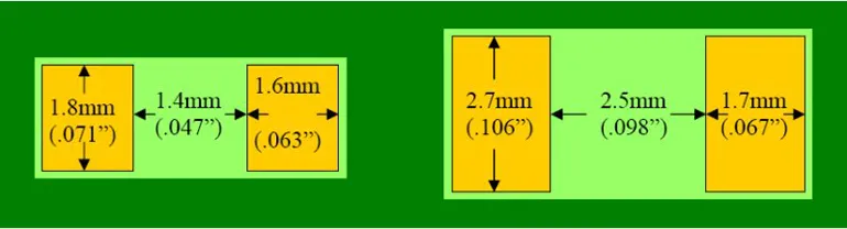
Figure 2. 1206 Pads
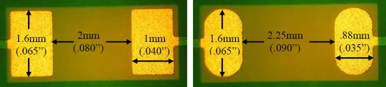
Figure 3. 1808 Pads
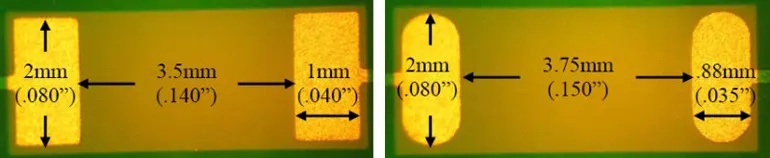
Table 1 is a summary of pad or land separation (creepage) for IPC 7351 designs, commonly encountered HV rectangular pads and oval pads with maximum separation.
| Case Size | IPC 7351 | HV Rectangular Pads | HV Oval Pads |
| 1206 | 1.4mm (0.047") | 2mm (0.080") | 2.25mm (0.090") |
| 1808 | 2.5mm (0.098") | 3.5mm (0.140") | 3.75mm (0.150") |
Test Capacitors
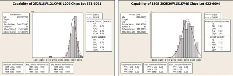
Production 150pF X7R 1808 parts and 120pF 1206 parts were pulled from inventory for use in these experiments. 2.5kV DC rated 1206 capacitors were used for the small case size and a 3kV rated 1808 safety capacitors were mounted on those pads. Eighty piece AC breakdown distributions for both parts are shown in Figure 4. The lower set limit or LSL is a 10% guard band above the 1500VAC test voltage used in product testing to insure parts mounted to assemblies pass using different test equipment in various customer facilities around the world.
Figure 4. AC Breakdown Distribution for the Chip Capacitors Used
Test Results
Table 2 summarizes 80 piece test results for each pad design variation (4) and test conditions including boards as received, bare chips, boards with parts reflow soldered with no-clean SAC lead free solder paste and exposed to 72 hours of 85%RH @ 85°C.The latter boards were tested for AC breakdown within an hour of removal from the 85/85 chamber.
| Pad Types | Bare Boards | Capacitors Not Mounted | Caps w/SAC | Caps w/SAC 85/85 |
| 1206 Chip Case Size | 3601VAC | |||
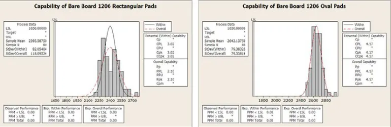
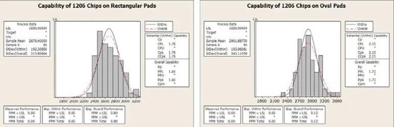
| Typical Square Pads | 2393VAC | 2676VAC | 2736VAC | |
| HV Rounded Pads | 2642VAC | 2901VAC | 3022VAC | |
| 1808 Chip Case Size | 3341VAC | |||
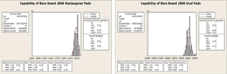
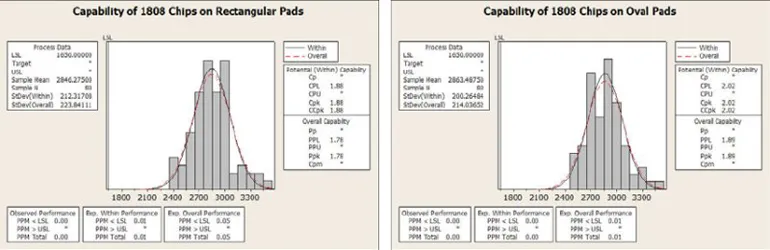
| Typical Square Pads | 3477VAC | 2846VAC | 2734VAC | |
| HV Rounded Pads | 4050VAC | 2863VAC | 2767VAC |
Conclusions
The impact of radius corners and increased creepage distance was most pronounced on the 1206 case sized chips with a 200V + increase in breakdown voltage for bare boards, chips mounted on boards and chips on boards after humidity exposure. An interesting side note was that breakdown voltages increased on 1206 case sized parts after being mounted on the boards with or without humidity exposure. The experiments were repeated with the same results.
The effect on the larger case size was not significantly different enough to take note of. Perhaps there is a threshold creepage distance that is between 1206 and 1808 case sizes where increases beyond that distance yields diminishing returns but that was beyond the scope of this study.
References
1) Maxwell, Lemus, E. "Arc Season and Board Design Observations"
Appendix 1. AC Breakdown Distributions
Bare Board Breakdown Capability 1206 Pads
Bare Board Breakdown Capability 1808 Pads
1206 Chip Capacitors Mounted on Boards as Soldered Breakdown Capability
1808 Chip Capacitors Mounted on Boards as Soldered Breakdown Capability
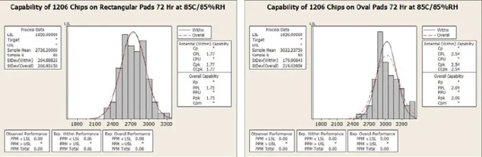
1206 Chip Capacitors Mounted on Boards Breakdown Capability after 72 Hours of 85°C/85%RH Exposure
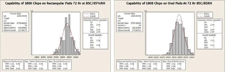
1808 Chip Capacitors Mounted on Boards Breakdown Capability after 72 Hours of 85°C / 85% RH Exposure
Notice: Specifications are subject to change without notice. Contact your nearest Johanson Dielectrics Sales Office for the latest specifications. All statements, information and data given herein are believed to be accurate and reliable, but are presented without guarantee, warranty, or responsibility of any kind, expressed or implied. Statements or suggestions concerning possible use of our products are made without representation or warranty that any such use is free of patent infringement and are not recommendations to infringe any patents. The user should not assume that all safety measures are indicated or that other measures may not be required. Specifications are typical and may not apply to all applications.