Johanson Dielectrics Solder Reflow Recommendations for Lead-free Assembly
General
Soldering temperature profiles used must provide adequate temperature rise time and cool-down time to prevent damage due to thermal shock. These guidelines are emphasized because cracking or other damage caused by handling or thermal shock is not very small (micro-cracks) and can occur under the terminations where even high magnification cannot detect them. The problem is further complicated by the fact that these micro-cracks may not be initially detectable by standard electrical testing. Once initiated, the cracks can grow with time and cause latent failures. Attention to these details will aid in the successful use of the inherently reliable multilayer ceramic capacitor.
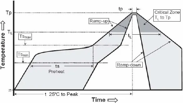
Ceramic capacitors larger then EIA size 1812 are known to be very susceptible to thermal shock damage due to their large ceramic mass. These large parts require more care during installation than smaller surface mount devices. Higher temperatures are now required for "Lead Free" solder profiles. The attached diagram from J-STD-020C shows both standard and lead free profiles.
| Profile Feature | Sn-Pb Eutectic Assembly | Pb_Free Assembly |
|---|---|---|
| Average Ramp-Up Rate (Tsmax to Tp) | 3° C / second max. | 3° C / second max. |
| Preheat: - Temperature Min (Tsmin) - Temperature Max (Tsmax) - Time (tsmin to tsmax) | 100° C 150° C 60 - 120 seconds | 150° C 200° C 60 - 180 seconds |
| Time maintained above: - Temperature (TL) - Time (tL) | 183° C 60 - 150 seconds | 217° C 60 - 150 seconds |
| Peak / Classification Temperature (Tp) | See Table 4.1 | See Table 4.2 |
| Time within 5° C of actual Peak Temperature (tp) | 10 - 30 seconds | 20 - 40 seconds |
| Ramp-Down Rate | 3° C / second max. | 3° C / second max. |
| Time 25° C to Peak Temperature | 6 minutes max. | 8 minutes max. |
Note 1: All temperature refer to topside of the package, measured on the package body surface.
Table 1
Solder Pre-Heat Cycle:
Proper preheating is essential to prevent thermal shock cracking of the capacitor. The circuit assembly should be preheated as shown in the recommended profiles at a rate of 1.0 to 3.0° C per second to within 75 to 125° C of the maximum soldering temperature. Temperature change should be distributed as evenly as possible throughout large capacitor bodies as applying heat or cold to a localized spot within device may result in thermal gradients great enough to cause cracking.
SMT Reflow Soldering Temperature
Solders typically utilized in SMT Reflow Solders have melting points between 179° C and 217° C. Activation of rosin fluxes occurs at about 200° C. Based on these facts reflow temperatures between 210 to 260° C should be adequate in most circumstances. Use of thermal profiling is advised for accurate characterization of circuit heat absorption and maximum component temperature conditions that occur during the soldering process.
Solder Reflow
Recommended temperature profiles for reflow soldering are shown in Table 1 and Figure 1 from J-STD-020C
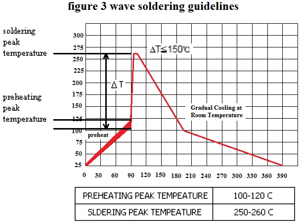
Solder Wave
Solders typically utilized in the solder wave have melting points between 179° C and 227° C. Wave soldering can be utilized for lead free assembly, but the preheat requirements generally make this process very difficult to accomplish as peak temperatures may reach 260° C. It is important that the preheat temperature is within 150° C of the solder wave peak temperature. And the maximum tie at peak temperature should not be greater than 5 seconds. Wave soldering is not recommended for ceramic MLCCs larger then 1206 and thicker than 1.2mm size due to the incompatibility of the chip's mass with the steep temperature gradient typically present in this process. Cool down after solder wave requires rate control < 2° C / sec.
Land patterns should be 2/3 narrower than the chip width to control solder fillet volume and minimize local Coefficient of Thermal Expansion (CTE) mismatch between the capacitor, solder and board.
Soldering Iron
Ceramic capacitor attachment with a soldering iron is discouraged due to the inherent process control limitations. In the event that a soldering iron must be employed the following precautions are recommended.
- Preheat circuit and capacitors to within 100° C of soldering temperature
- Never contact the capacitor with the iron tip
- 20 watt iron output (max)
- 350° C tip temperature (max)
- 1.0 mm tip diameter (max)
- Limit soldering time to 3 sec.
Cool Down Cycle
After the solder reflows properly the assembly should be allowed to cool gradually, again maintaining the thermal gradient of 3° C / sec. maximum at room ambient conditions. Attempts to speed this cooling process or immediate exposure of the circuit to cold cleaning solutions increase the possibility of thermal shock cracking of the ceramic capacitor.
Ceramic capacitor attachment with a soldering iron is discouraged due to the inherent process control limitations. In the event that a soldering iron must be employed the following precautions are recommended.
IPC 7351 Land Pattern Guidelines
Appropriate pad design, solder application, and component orientation are all ingredients of a quality, defect-free soldering process. The Institute for Interconnecting and Packaging Electronic Circuits (IPC) has developed and published IPC 7351 "Surface Mount Design and Land Pattern Standard". This standard presents industry consensus on optimum dimensions based on empirical knowledge of fabricated land patterns. The standard also contains an excellent analysis of solder joints and their relation to component, PCB, and placement tolerances. A summary of the IPC land pattern design recommendations for solder reflow and solder wave processes are listed in table below. It is highly recommended that the PCB designer/SMT process engineer obtain the complete IPC 7351 standard.
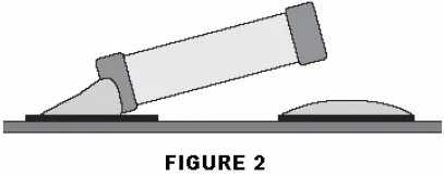
Tomb Stoning / Chip Movement
Tomb-stoning or draw bridging is illustrated in figure 2. Tomb-stoning or other undesirable chip movements may result if unequal surface tension forces exist as the molten solder wets the MLCC terminations and mounting pads. This tendency can be minimized by insuring that all factors at both solder joints are equal, namely; pad size, solder mass, termination size, component position and heating. Tomb-stoning is easily avoided through proper design, material selection, control of solder mass and proofing of the process.
Notice: Specifications are subject to change without notice. Contact your nearest Johanson Dielectrics, Inc. Sales Office for the latest specifications. All statements, information and data given herein are believed to be accurate and reliable, but are presented without guarantee, warranty, or responsibility of any kind, expressed or implied. Statements or suggestions concerning possible use of our products are made without representation or warranty that any such use is free of patent infringement and are not recommendations to infringe any patents. The user should not assume that all safety measures are indicated or that other measures may not be required. Specifications are typical and may not apply to all applications.