EMI Filter Evaluation and PCB Design Guide
By Steve Cole - EMI Product Mgr. Johanson Dielectrics, Inc Mar. 18, 2009
EMI IN A NUTSHELL (Basic Theory)
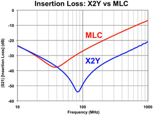
EMI is an ultra-low inductance 3-node capacitor circuit consisting of two balanced Y capacitors of equal value. This configuration enables filtering of two signal lines (or positive AND negative power lines) simultaneously. A special electrode design provides broadband filtering characteristics for both differential and common-mode noise signals into the GHz band. EMI Immunity and Radiated Emissions performance far exceeds that of standard ceramic MLCs and multi-component filters. X2Y’s low inductance maintains insertion loss over a wide frequency band, not just a narrow bandwidth around the capacitor SRF. This means that for a given capacitance value and corresponding pass band Fc, X2Y’s deliver far better high frequency filtering then standard MLCs.
IDENTITY CRISIS (EMI vs. Feed-Thru Filter)
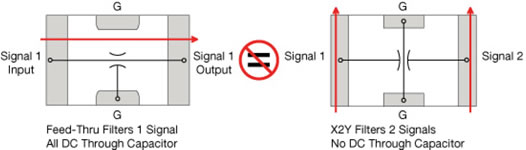
Externally an EMI® closely resembles a chip feed-thru EMI filter but has major internal, schematic, and performance differences. A feed-thru capacitor drives one filtered signal through the capacitor along the long component axis and must handle both DC current and AC noise currents. EMI capacitors filter two signal lines simultaneously shunting only noise. Since no DC currents flow through the EMI, there is no DC current limitation. (In EMI applications AC noise currents are orders of magnitude smaller than DC currents.)
HIT THE GROUND RUNNING (EMI Connection Options)
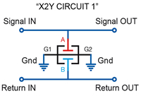
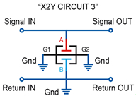
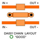
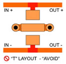
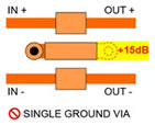
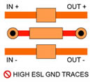
EMI capacitors require a low inductance, dual ground connection as seen in “Circuit 1.” Chassis or system ground is preferred, but if unavailable, an isolated or “floating” ground may be used very effectively. Because the filtered noise currents are small, adding a copper flood layer in the PCB and connecting it with vias to G1 & G2 create an image plane. Circuit 3 may be used in applications where a signal line is common with system ground. Comparative radiated emissions testing shows nearly the same level of effectiveness.
NO-FLY ZONE (Minimize Connection Inductance)
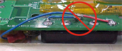
Fly-wire connections introduce large blocking inductances that do not work in EMC applications. For best results use an EMI specific layout for evaluations per the PCB Layout Guide. If this isn’t possible make every attempt to make a well-grounded, low inductance placement. Occasionally EMI can be kludged to an existing PCB for testing by careful cutting or exposing traces and/or addition of copper foil or braid. Such kludges should follow basic EMC design principals and have minimal inductance for effective EMI filtering.
WHERE’S THE BEEF? (PCB Layout Guidelines)
Component specific terminal pad dimensions are listed in the JDI EMI datasheet. PCB via layout dimensions depend on PCB fabrication and assembly capabilities. Use of solder mask beneath component is NOT recommended
LOCATION, LOCATION, LOCATION (Preventing EMI Coupling)
- For EMI Immunity, unshielded enclosures:
- EMI should be located as close to sensitive IC (e.g. amplifier) inputs as possible.
- Vcc should also be decoupled by EMI.
- For EMI Radiation, unshielded enclosures:
- EMI should be applied as close to the PCB input/output/power entry/exit point as possible.
- For EMI Radiation/Immunity, shielded enclosures:
- EMI G1/G2 connections should be as low inductance as possible to the case bulkhead, or an image plane tightly coupled to the case bulkhead, close to signal input / output.
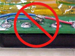
AVOID CRACK-UPS (Lab Soldering Precautions)
Ceramic capacitors (EMI and standard MLC types) can be easily damaged when hand soldered. Thermal cracking of the ceramic body is often invisible even under a microscope. Factors that increase thermal cracking risk:
- 4 terminals to solder can increase hand-soldering time
- Pb-free solders have higher reflow temperatures
- Low inductance connections to ground are inherently good heat-sinks
A damaged component may exhibit a short circuit immediately and not recover, or may operate with intermittent Insulation Resistance (IR) levels. If you are not achieving expected results and have followed the other guidelines carefully, check to see you are adhering to the soldering guidelines below:
- Always pre-heat the PCB and component to within 50°C of solder reflow temperature at 2°C/sec. maximum.
- Use contact-less hand solder tools such as a hot air pencil, IR lamp, etc.
- Use a soldering iron as last resort; 20W max. tip, NO CONTACT with ceramic, limit solder time to 20 secs.
A reliable, cost effective prototype PCB reflow soldering process is possible using a household toaster oven. There are several good procedures available on-line by googling “Toaster Oven Soldering”
SUMMARY OF CRITICAL GUIDELINES
- Use the best circuit connection option for the application
- Provide the lowest inductance connections to the PCB
- Connect BOTH component ground terminals in the circuit to lower inductance.
- Apply EMI components in the most effective PCB location
- Use reliable soldering practices to avoid component damage and electrical degradation
A HELPING HAND (EMI Design Assistance Available)
There are many detailed EMI application notes available on this site. We encourage you to involve us early in you design evaluation of EMI technology. If you’ve followed these guidelines and still aren’t getting the results you expect, we’d like to hear from you. Please contact us with your test data and close-up pictures of your PCB.