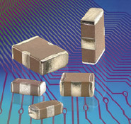
EMI Filter & Decoupling Capacitors
This is a Multilayer Ceramic device that combines two balanced shunt capacitors, with mutual inductance cancellation and shielding effect. When properly laid out, this monolithic broadband filter provides fantastic rejections for single-ended (e.g. power bypass) or differential configurations (e.g. modulated power and return of a brushed DC motor noise).
Used for both EMI filtering and noise attenuation, the component is an effective EMC solution for common mode noise issue, and it allows to get rid of differential noise as well. It can replace DC common mode chokes and provide better performances as an EMI filter or RFI filter. It can also replace Common Mode Chokes in many cases of RF interference or noise cancelling. This solution should be considered for all EMI noise suppression filters and for noise filtering.
Automotive version (AEC-Q200) available for many values: please see details in the below table of capacitance values. Please contact us if another value is needed for automotive application.
General Information
Applications:
- Amplifier FIlter & Decoupling
- High Speed Data Filtering
- EMC I/O Filtering
- FPGA / ASIC / μ-P Decoupling
- DDR Memory Decoupling
Advantages:
- One device for EMI suppression or decoupling
- Replace up to 7 components with one EMI
- Differential and common mode attenuation
- Matched capacitance line to ground, both lines
- Low inductance due to cancellation effect
Key Features:
- AEC-Q200 Automotive Qualification (as required)
Common Traits with Conventional MLCC:
- Same component sizes (0603, 0805, 1206, etc.)
- Same pick and place equipment
- Same voltage ratings
- Same dielectric, electrode and termination materials
- Same industry test standards for component reliability
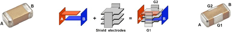
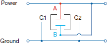
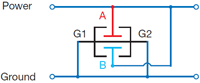
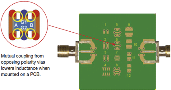
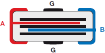
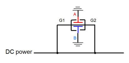
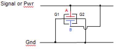
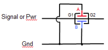
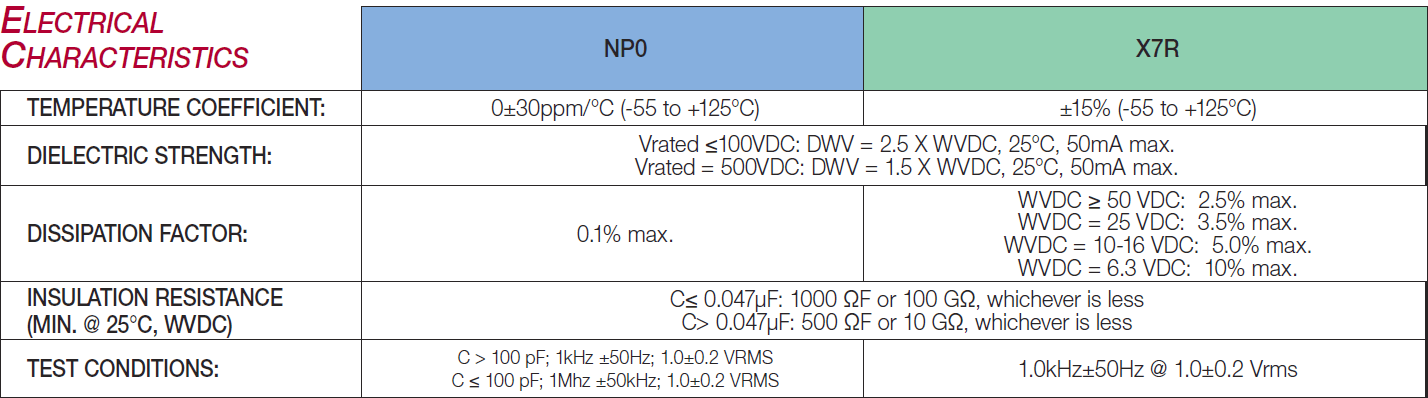
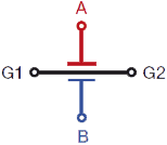
The EMI® capacitor design starts with standard 2 terminal MLC capacitor’s opposing electrode sets, A & B, and adds a third electrode set (G) which surround each A & B electrode. The result is a highly vesatile three node capacitive circuit containing two tightly matched, low inductance capacitors in a compact, four-terminal SMT chip.
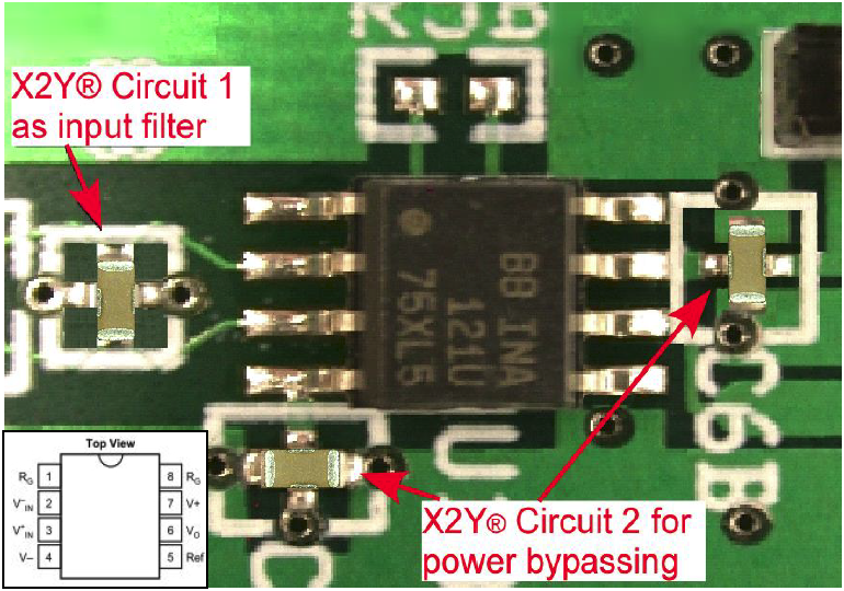
EMI Filtering:
The EMI® component contains two shunt or “line-to-ground” Y capacitors. Ultra-low ESL (equivalent series inductance) and tightly matched inductance of these capacitors provides unequaled high frequency Common-Mode noise filtering with low noise mode conversion. EMI® components reduce EMI emissions far better than unbalanced discrete shunt capacitors or series inductive filters. Differential signal loss is determined by the cut off frequency of the single line-to-ground (Y) capacitor value of an EMI®.
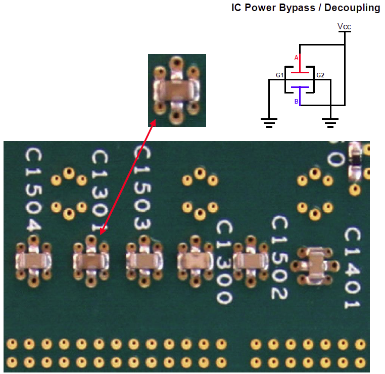
Power Bypass / Decoupling
For Power Bypass applications, EMI's® two “Y” capacitors are connected in parallel. This doubles the total capacitance and reduces their mounted inductance by 80% or 1/5th the mounted inductance of similar sized MLC capacitors enabling high-performance bypass networks with far fewer components and vias. Low ESL delivers improved High Frequency performance into the GHz range.
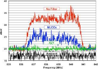
GSM RFI Attenuation in Audio & Analog
GSM handsets transmit in the 850 and 1850 MHz bands using a TDMA pulse rate of 217Hz. These signals cause the GSM buzz heard in a wide range of audio products from headphones to concert hall PA systems or “silent” signal errors created in medical, industrial process control, and security applications. Testing was conducted where an 840MHz GSM handset signal was delivered to the inputs of three different amplifier test circuit configurations shown below whose outputs were measured on a HF spectrum analyzer.
- No input filter, 2 discrete MLC 100nF power bypass caps.
- 2 discrete MLC 1nF input filter, 2 discrete MLC 100nF power bypass caps.
- A single EMI 1nF input filter, a single EMI 100nF power bypass cap.
EMI configuration provided a nearly flat response above the ambient and up to 10 dB imrpoved rejection than the conventional MLCC configuration.
Capacitance Values
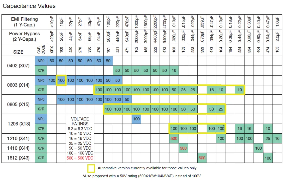
 Automotive version currently available for those values only
*Also proposed with a 50V rating (500X18W104MV4E) instead of 100V
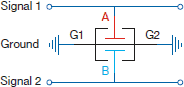
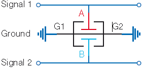
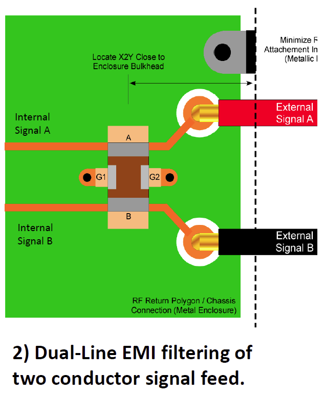
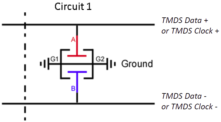
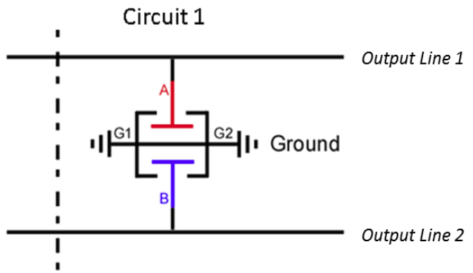
EMI Circuit 1: Filtering
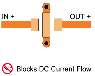
When used in circuit 1 configuration the EMI® filter capacitor is connected across two signal lines. Differential mode noise is filtered to ground by the two Y capacitors, A & B. Common mode noise is cancelled within the device.
Experts agree that balance is the key to a "quiet" circuit. EMI® is a balanced circuit device with two equal halves, tightly matched in both phase and magnitude with respect to ground. Several advantages are gained by two balanced capacitors sharing a single ceramic component body.
- Exceptional common mode rejection
- Effects of aging & temperature are equal on both caps
- Effect of voltage variation eliminated
- Matched line-to-ground capacitance
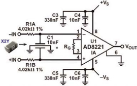
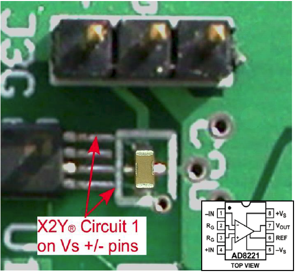
Amplifier Input Filter Example
In this example, a single Johanson EMI® component was used to filter noise at the input of a DC instrumentation amplifier. This reduced component count by 3-to-1 and costs by over 70% vs. conventional filter components that included 1% film Y-capacitors.
| Parameter | EMI® 10nF | Discrete 10nF, 2@220 pF | Comments |
|---|---|---|---|
| DC offset shift | < 0.1 µV | < 0.1 µV | Referred to input |
| Common mode rejection | 91 dB | 92 dB |
Source: Analog Devices, “A Designer’s Guide to Instrumentation Amplifiers (2nd Edition)” by Charles Kitchin and Lew Counts
Common Mode Choke Replacement
- Superior High Frequency Emissions Reduction
- Smaller Sizes, Lighter Weight
- No Current Limitation
- Vibration Resistant
- No Saturation Concerns
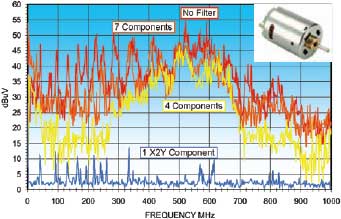
DC Motor EMI Reduction: A Superior Solution
One EMI® component has successfully replaced 7 discrete filter components while achieving superior EMI filtering.
Parallel Capacitor Solution
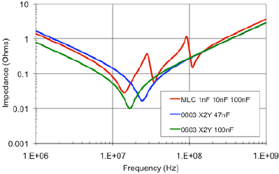
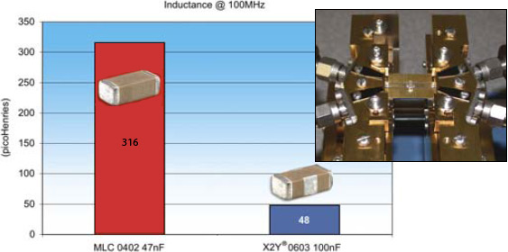
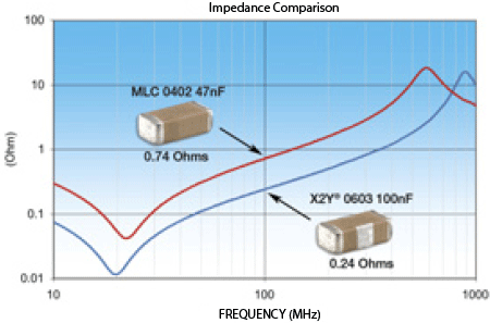
A common design practice is to parallel decade capacitance values to extend the high frequency performance of the filter network. This causes an unintended and often over-looked effect of anti-resonant peaks in the filter networks combined impedance. EMI’s very low mounted inductance allows designers to use a single, higher value part and completely avoid the anti-resonance problem. The impedance graph on right shows the combined mounted impedance of a 1nF, 10nF & 100nF 0402 MLC in parrallel in RED. The MLC networks anti-resonance peaks are nearly 10 times the desired impedance. A 100nF and 47nF EMI are plotted in BLUE and GREEN. (The total capacitance of EMI (Circuit 2) is twice the value, or 200nF and 98nF in this example.) The sigle EMI is clearly superior to the three paralleled MLCs.
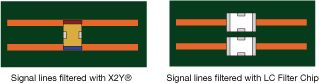
Signal Line Filter for USB & RJ45
One EMI® component can effectively filter high speed signal lines replacing replacing multiple inductive and ferrite components.
Other EMI® Filter Applications
DC-DC converters, power I/O, connectors (RJ45, D-sub), audio/voice/data, CAN, high-speed differential.
Effectively replaces common mode chokes, inductors, ferrites and feedthru capacitors.
Power Bypass
EMI® Circuit 2: Decoupling
When used in circuit 2 configuration, A & B capacitors are placed in parallel effectively doubling the effective capacitance while maintaining an ultra-low inductance. The low inductance advantages of the EMI® Capacitor Circuit enables high-performance bypass networks at reduced system cost.
- Lower via count, improves routing
- Reduces component count
- Lowers placement cost
- Low ESL (device only and mounted)
- Broadband Performance
- Effective on PCB or package
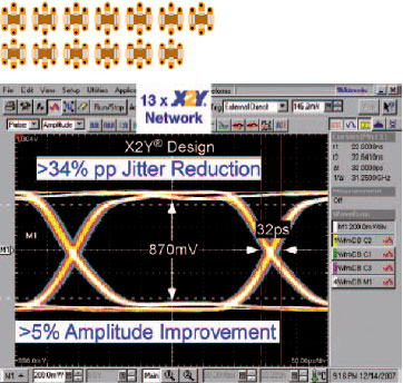
EMI High Performance Power Bypass - Improve Performance, Reduce Space & Vias
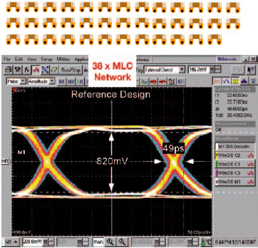
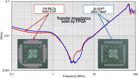
Actual measured performance of two high performance SerDes FPGA designs demonstrate how a 13 component EMI bypass network significantly out performs a 38 component MLC network.
Component Performance
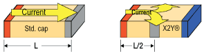
The EMI® has short, multiple and opposing current paths resulting in lower device inductance
PCB MOUNTED PERFORMANCE
SYSTEM PERFORMANCE
1:5 MLCC REPLACEMENT EXAMPLE
EMI's proven technology enables end-users to use one EMI capacitor to replace five conventional MLCCs in a typical high performance IC bypass design. Vias are nearly cut in half, board space is reduced and savings are in dollars per PCB.
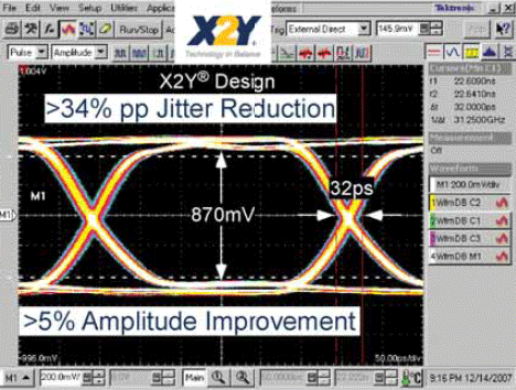
34% NOISE IMPROVEMENT 1:3 MLCC REPLACEMENT
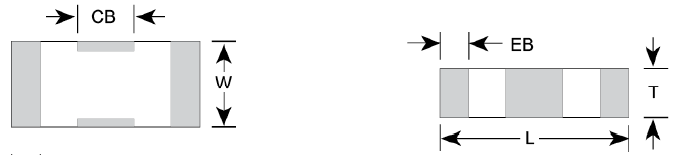
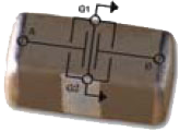
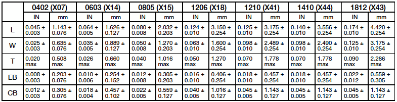
EMI Component & Pad Sizes
| Physical Dimensions |
0402 (X07) | 0603 (X14) | 0805 (X15) | 1206 (X18) | 1210 (X41) | 1410 (X44) | 1812 (X43) | ||||||||
|---|---|---|---|---|---|---|---|---|---|---|---|---|---|---|---|
| IN | mm | IN | mm | IN | mm | IN | mm | IN | mm | IN | mm | IN | mm | ||
| Chip | L | 0.045 ±.003 |
1.143 ±.076 |
0.064 ±.005 |
1.626 ±.127 |
0.080 ±.008 |
2.032 ±.203 |
0.124 ±.010 |
3.150 ±.254 |
0.125 ±.010 |
3.175 ±.010 |
0.140 ±.010 |
3.556 ±.254 |
0.174 ±.010 |
4.420 ±.254 |
| W | 0.025 ±.003 |
0.635 ±.076 |
0.035 ±.005 |
0.889 ±.127 |
0.050 ±.008 |
1.270 ±.203 |
0.063 ±.010 |
1.600 ±.254 |
0.098 ±.010 |
2.489 ±.254 |
0.098 ±.010 |
2.490 ±.254 |
0.125 ±.010 |
3.175 ±.254 |
|
| T | 0.020 max. |
0.508 max. |
0.026 max. |
0.660 max. |
0.040 max. |
1.016 max. |
0.050 max. |
1.270 max. |
0.070 max. |
1.778 max. |
0.070 max. |
1.778 max. |
0.090 max. |
2.286 max. |
|
| EB | 0.008 ±.003 |
0.203 ±.076 |
0.010 ±.006 |
0.254 ±.152 |
0.012 ±.008 |
0.305 ±.203 |
0.016 ±.010 |
0.406 ±.254 |
0.018 ±.010 |
0.457 ±.254 |
0.018 ±.010 |
0.457 ±.254 |
0.022 ±.012 |
0.559 ±.305 |
|
| CB | 0.012 ±.003 |
0.305 ±.076 |
0.018 ±.004 |
0.457 ±.102 |
0.022 ±.005 |
0.559 ±.127 |
0.040 ±.005 |
1.016 ±.127 |
0.045 ±.005 |
1.143 ±.127 |
0.045 ±.005 |
1.143 ±.127 |
0.045 ±.005 |
1.143 ±.127 |
|
| Solder Pad | X | 0.020 | 0.51 | 0.035 | 0.89 | 0.050 | 1.27 | 0.065 | 1.65 | 0.100 | 2.54 | 0.100 | 2.54 | 0.125 | 3.18 |
| Y | 0.018 | 0.45 | 0.025 | 0.64 | 0.035 | 0.89 | 0.040 | 1.02 | 0.040 | 1.02 | 0.040 | 1.02 | 0.040 | 1.02 | |
| G | 0.028 | 0.71 | 0.040 | 1.02 | 0.050 | 1.27 | 0.080 | 2.03 | 0.080 | 2.03 | 0.100 | 2.54 | 0.130 | 3.30 | |
| V | 0.013 | 0.33 | 0.020 | 0.51 | 0.022 | 0.56 | 0.040 | 1.02 | 0.045 | 1.14 | 0.045 | 1.14 | 0.045 | 1.14 | |
| U | 0.039 | 0.99 | 0.060 | 1.52 | 0.080 | 2.03 | 0.120 | 3.05 | 0.160 | 4.06 | 0.160 | 4.06 | 0.190 | 4.83 | |
| Z | 0.064 | 1.63 | 0.090 | 2.29 | 0.120 | 3.05 | 0.160 | 4.06 | 0.160 | 4.06 | 0.180 | 4.57 | 0.210 | 5.33 | |
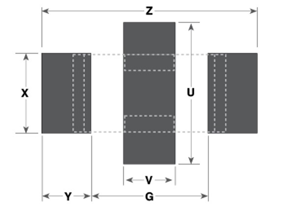
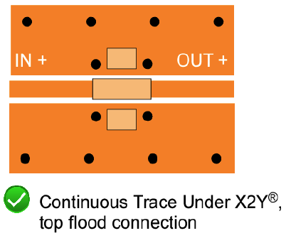
Solder mask beneath component should be avoided or minimized to reduce flux & containment entrapment
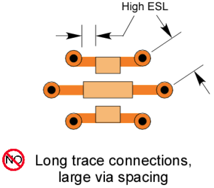
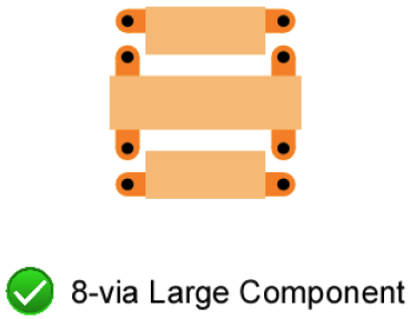
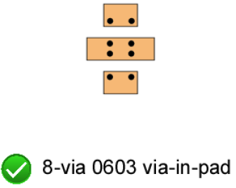
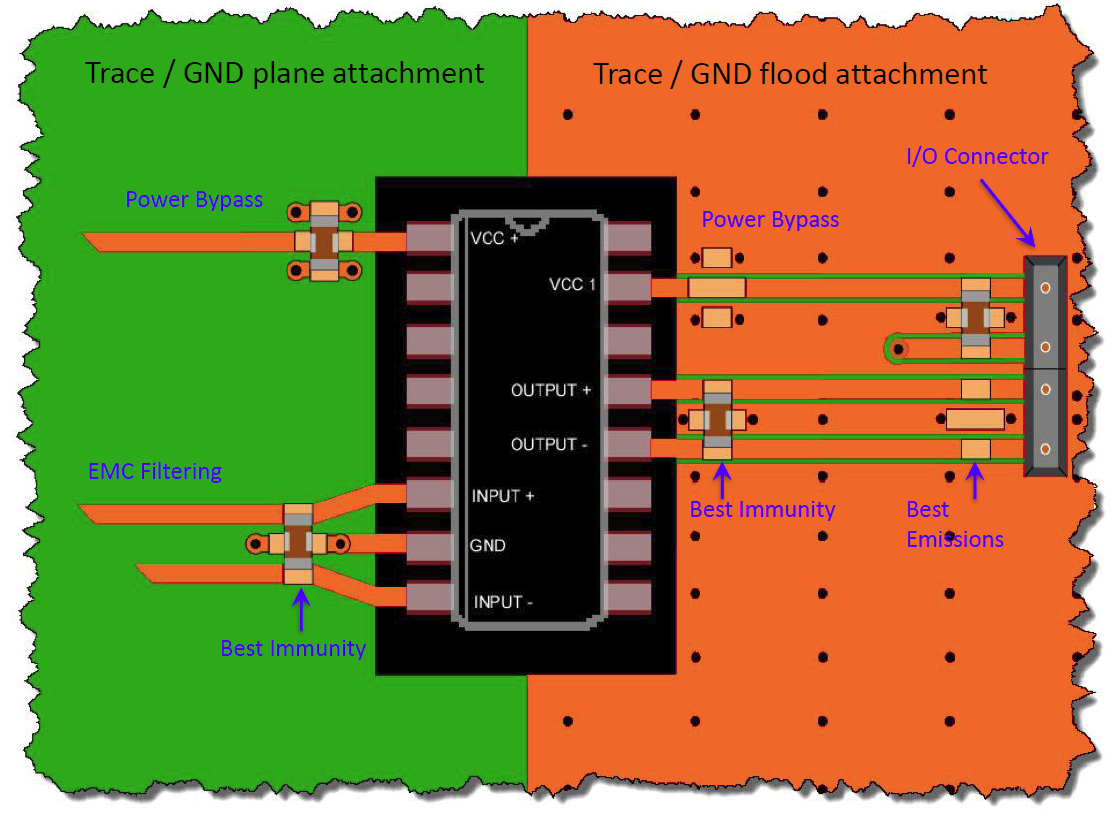
Trace - Via Layout Summary
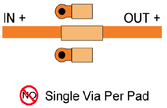
The following are key elements of Good Mounting Practice when applying EMI components with traces and vias on the PCB.
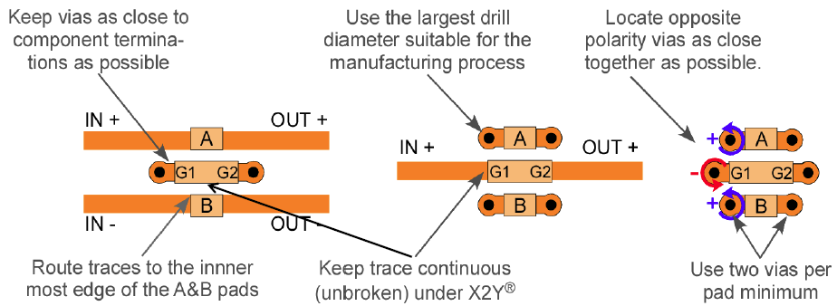
Differential configuration - Trace & Via Layouts
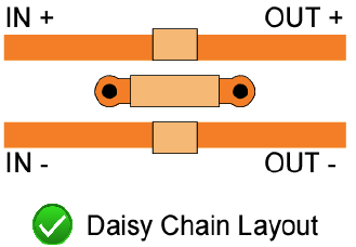
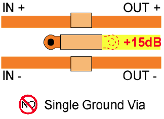
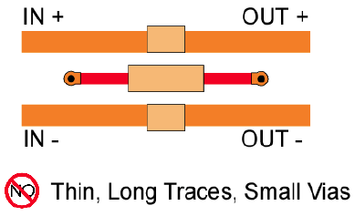
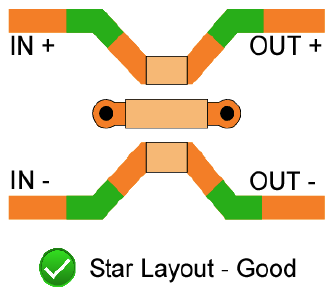
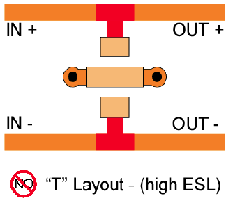
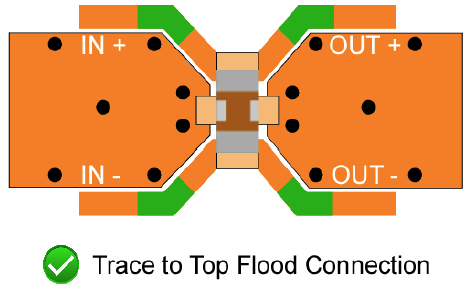
Single-Ended Configuration - Trace & Via Layouts


Examples 1, 2: Dual-Line EMI Filtering
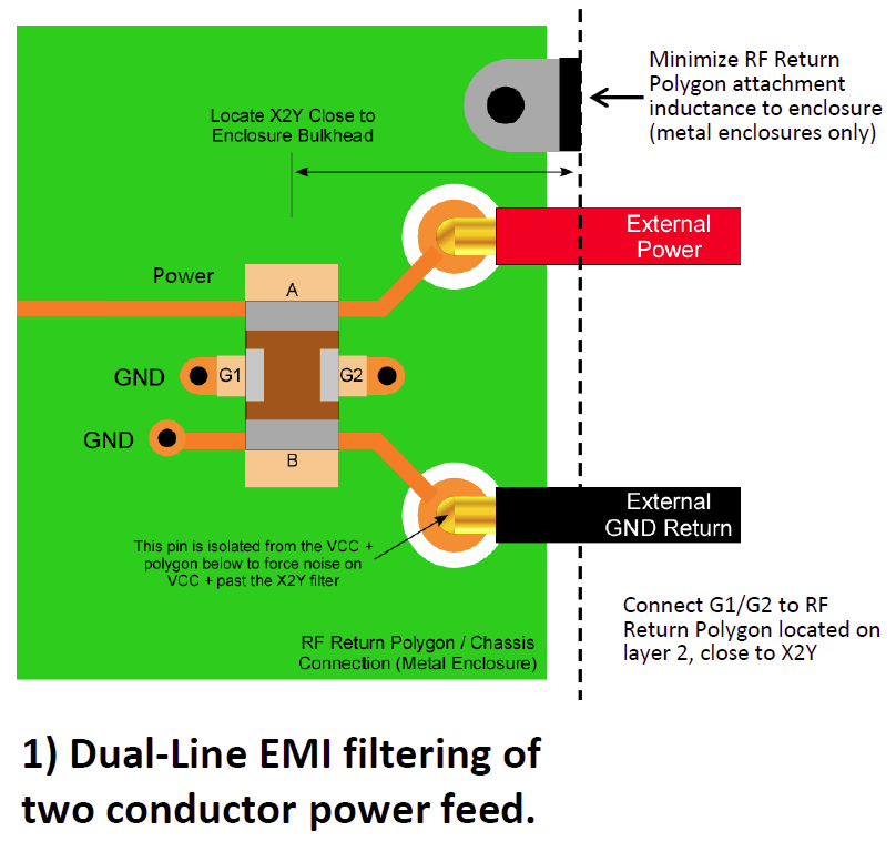
Examples 4,5: Dual Line EMI Filtering
Signal Cable I/O
Power and Signal Cable I/O
Example 6: EMI Filter & Power Bypass
IC +/- power pins on same side: Single EMI replaces 4 MLCCs, bypassing both the power rails.
EMI applied as dual-line input filter. IC +/- power pins on opposite sides, EMI is applied in bypass on each power rail.
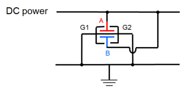
IC Power Bypass: Inner Planes Attachment
Multiple EMI components are attached between the inner Vcc an GND planes on this PCB for FPGA power bypassing.
IC & Connector Pin Placement
IC Power Bypass : Reduced EMC
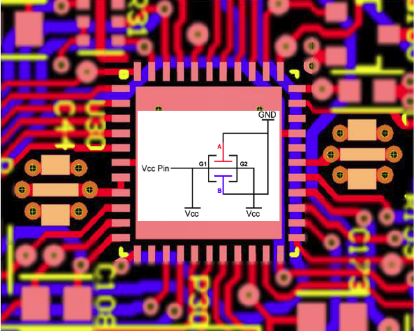
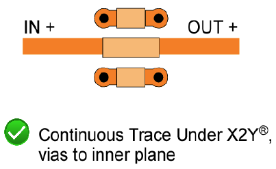
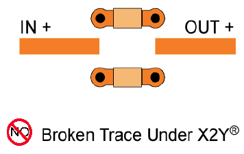
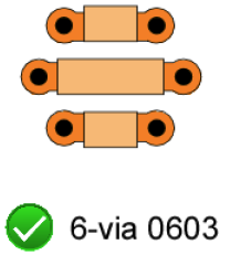
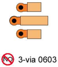
Using 6-vias and a continuous trace under the EMI results in the lowest PDN impedance to GND.
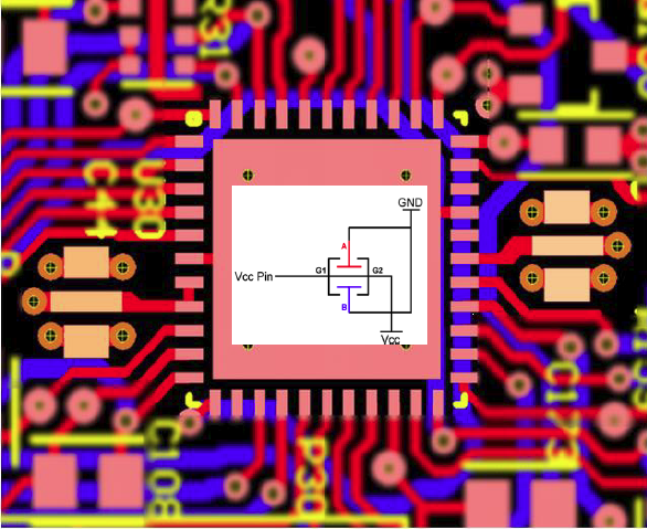
Using 5-vias, removing via between the IC pin and EMI, maximizes RF noise immunity. All noise must first go through the EMI filter before reaching the IC power pin.
We're here to help
Johanson provides first time adopters with application engineering assistance including part selection, schematic design review and PCB layout review.
Contact your local field sales representative for more information.
Thank You for your interest in the EMI Solution
Electrical Specifications
Mechanical Specifications
How to Order
Valid options are shown except for Capacitance
A typical PN is EMCP160W224M1GV001T. This part number breaks down as follows:
Capacitors Surface Mount PME < 500V, 1812, X7R, 250.0V, 0.01µF±5%, Ni/Sn (RoHs), Bulk
New Johanson Global Part Number Breakdown
* Not all combinations create valid part numbers, ask our Apps Engineering Team for assistance creating a valid part number Request for assistanceClick below to see the new Global Part Number Reference Chart for this product
Legacy How to Order Information