EMI Power Bypass PCB Mounting
Get the Most from EMI Capacitors with Proper Attachment Techniques
Summary
EMI capacitors excel in low inductance performance for a myriad of applications including EMI/RFI filtering, power supply bypass / decoupling. How the capacitor attaches to the application PCB is every bit as important as the capacitor itself. This application note demonstrates recommended attachment practices.
Introduction
Capacitor performance, and particularly, low inductance capacitor performance can depend heavily on the pad layout and via attachment patterns. Proper attention to layout issues insures top device performance.
Loop Inductance
Inductance always evaluates around a loop. Bypass capacitor mounted inductance is a function of the entire physical path(s) from the capacitor load through all interconnects. Best results are obtained by minimizing the loop area. Figure 1 illustrates the inductance loop for a bypass capacitor attached to planes well within a PCB. L1 represents the inductance of the capacitor with a specific land and via pattern. L2 represents the incremental inductance associated with a given via pattern and depth to the near plane in a power / ground cavity. Proper attachment techniques maximize capacitor performance by minimizing the L1and L2 inductances.
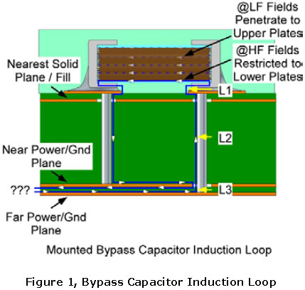
Additionally, bypass capacitor inductance is not constant with frequency. Internally, bypass capacitor plates create shields that limit high frequency penetration away from the mounting surface. This reduces inductance at high frequencies, ( > 50-100MHz ).
The cardinal rules of high performance land patterns:
- Limit solder pads to only as large as necessary for good manufacturability
- Locate vias as close to device terminals as possible.
- Use the largest drill diameter suitable for the manufacturing process
- Locate opposite polarity vias as close together as possible.
- Understand the difference between finished PTH hole size and drilled hole diameter
- Locate a solid plane or power patch as close to the capacitor surface as possible
- Locate high performance planes close to the capacitor mounting surface
- Always locate capacitors on the PCB surface closest to the planes they support.
Rule #1
Limit Pad Sizes. Limiting capacitor pad sizes helps to move vias closer to the device terminals and reduce inductance. Pad sizes should be chosen to allow for good solderability. Reflow soldering tolerates smaller pads than wave soldering. Reflow is preferred for low inductance. Pad extension beyond the component of 10mils is typically more than adequate to form a high quality solder meniscus.
Rule #2
Locate Vias as Close to Device Terminals as Possible. Vias should locate only as far from the capacitor as necessary to allow for solder mask dam and via clearance. Modern manufacturing typically supports a solder mask dam with a10 mil diameter annular ring over the finished hole, IE 5 mil radius over finished hole radius.
Rule #3
Use the Largest Drill Diameter Suitable for the Manufacturing Process. The ratio of the outside via hole diameter to the center to center spacing determines self inductance for each via pair. Particularly for planes buried deep within a board optimizing vias affords significant gains. Via drill diameter should be chosen as large as possible without:
- Unduly pushing vias away from capacitor terminals
- Unduly blocking signal routing channels
- Unduly causing large plane perforations
At the same time that larger vias reduce the induction loop size inside the PCB, minimum edge to edge solid material requirements dictates pushing vias apart asthey grow. This slowly increases mounted inductance due to the longer path on the capacitor surface of the PCB. Additionally, as vias grow, antipads should not be allowed to grow to the point that they run together.
Rule #4
Locate Opposite Polarity Vias as Close Together as Possible. Just as maximizing tolerable the ratio of via diameter to center-to-center spacing determines self inductance by a log arithmic relationship. With smaller EMI capacitors, locating the vias as close to the device as possible also tends to minimize distance between vias. On larger EMI parts, eight via patterns should be used, so as to create a via pair across each of the four device corners.
Rule #5
Understand the Difference Between Via Drill and Finished Hole Diameter. Most PCB houses specify finished hole diameter, and do so with a fairly wide tolerance, typically -.001/+.004 for vias. Finished hole diameters are important when they are used for through hole leads. Otherwise, they are popular because they can be verified. Whenever possible, find out from your fabrication vendor the actual drill size used for each common diameter hole. Then adjust the fabrication drawing to call out a drill diameter that meets manufacturability requirements for the selected board vendor(s). Be certain to communicate clearly to the vendor, when you want to specify a given drill, instead of just a finished hole size.
Rule #6
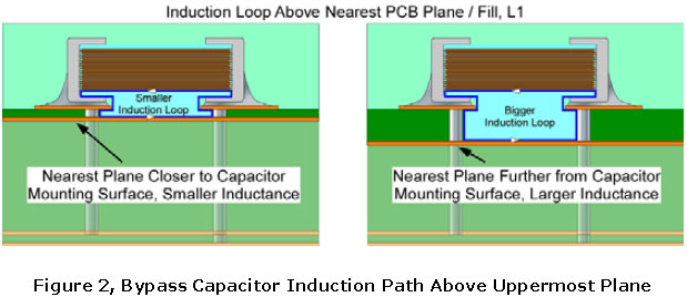
Locate Solid Fill / Plane Close to the Capacitor Mounting Surface. The L1 capacitor inductance is a function of the entire capacitor plus PCB feature geometry down to the first solid fill or plane that substantially surrounds the capacitor body. The plane / fill acts as shield. It does not matter what DC voltage is on the plane / fill, or even that it is connected to the capacitor. What matters is how close it is to the capacitor surface. L1 inductance is non-linear. Locating L1 within the first 10 mils or so of the surface does not have a major impact on capacitor performance. However, more than 10 mils down, L1 inductance increases very rapidly.
Rule #7
Locate High Performance Planes Close to the Cap Mounting Surface. Figure 1 illustrates components of attached capacitor inductance for planes buried deep within the printed circuit board. With EMI capacitors and a good vial ayout, the incremental inductance of the section marked L2 typically varies from 3.3pH to 4pH / mil of the L2 cavity, depending on the specific dimensions andl ocation of vias. A very poor layout can drive this value up over 5pH / mil.
As shown in Table 1, a power cavity on layers 6/7 requires one and half times as many capacitors as does a power cavity on layers 2/3 for the same impedance, while cavities on layers 10/11 require twice as many capacitors as layers 2/3.
Rule #8
Locate High Performance Planes Close to the Cap Mounting Surface. Always Locate Capacitors on the PCB Surface Closest to the Planes. Bypass capacitors that connect to planes in the upper half of the board stack-up should be mounted on the PCB top surface, while those that connect to planes in the bottom half should be mounted on the bottom. Table 1 demonstrates that the penalty for traversing to the opposite side of the board can require nearly 3.0 times as many capacitors at low frequency, and 3.5 times as many capacitors at high frequency as when the capacitors locate on the near mounting surface. The ratio diminishes as capacitors attach to low performance cavities closer to the middle of the PCB.
| Closer Plane Depth (Distance from capacitor mounting surface to closer of two planes in power cavity) | Typical Inductance | |
|---|---|---|
| LF | HF | |
| 5mils | 146pH | 118pH |
| 10mils | 166pH | 138pH |
| 15mils | 186pH | 158pH |
| 20mils | 206pH | 178pH |
| 25mils | 226pH | 198pH |
| 30mils | 246pH | 218pH |
| 35mils | 2666pH | 238pH |
| 40mils | 286pH | 258pH |
| 45mils | 306pH | 278pH |
| 50mils | 326pH | 298pH |
| 55mils | 346pH | 318pH |
| 60mils | 366pH | 338pH |
| 65mils | 386pH | 358pH |
| 70mils | 406pH | 368pH |
| 75mils | 426pH | 388pH |
| 80mils | 446pH | 408pH |
| 85mils | 466pH | 428pH |
| 90mils | 486pH | 448pH |
| 95mils | 506pH | 468pH |
| 100mils | 526pH | 488pH |
| 105mils | 546pH | 508pH |
| 110mils | 566pH | 528pH |
| 115mils | 586pH | 548pH |
Given so many variables that are application dependent, how do capacitor manufacturers obtain data sheet ESL values? The answer is that they first measure a reference value on a fixture with a shorting plate in place of the DUT¹. Then, they measure with a DUT, typically held to the surface under compression. Manufacturers report the measured difference as data sheet ESL.
It should be apparent that this measurement reports only the incremental inductance of the capacitor body over a shorted plate. It does not report the inductance of a capacitor in any application. As such, these values are useful primarily for qualitative comparison between like geometry and terminal configuration capacitors. In order to predict bypass capacitor performance in actual applications, we need to determine the inductance of the entire loop depicted in Figure 2.
EMI Preferred Layouts
EMI has developed preferred layouts based on common class II PCB manufacturing rules, and JEDEC rules for high assembly reliability.
EMI 0603 Recommended Reflow Layouts
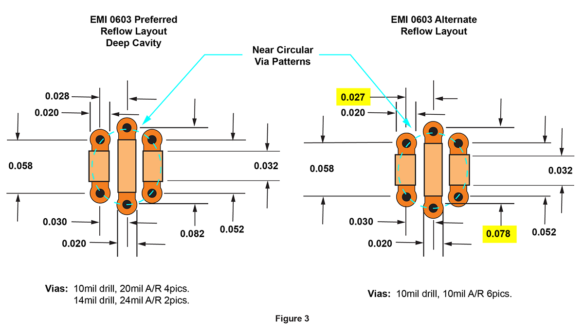
These layouts arrange pads for 10mils extension beyond capacitor terminals for good meniscus wicking. Vias push-out from the pads only by sufficient distance for reliable solder mask dams.
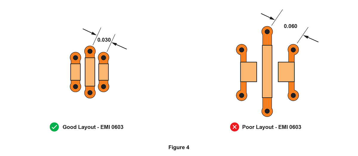
Perils of Poor Layouts
A good PCB layout optimizes via placements for the capacitor used and realizes superior performance. Poor PCB layouts squander performance, requiring more capacitors, and more vias to do the same job. Figure 4, compares the EMI recommended alternate layout against a poor layout. Because of its long extents from device terminals to vias, and the wide via separation, the poor layout shown performs badly. It exhibits approximately 200% L1 inductance, and 150% L2 inductance compared to recommended EMI layouts.
Comparative Layouts, EMI 0603
EMI Layouts, Large Capacitors
Ordinary capacitor construction dictates that device and via loop inductances both increase as larger bodies push the terminals and vias apart. The unique perpendicular design of the EMI capacitor avoids these problems, because the vias and terminal connections form in pairs around the corners in an eight via pattern, maintaining minimum size loops and maximum via utilization.
Figure 5 illustrates recommended layouts for 0805, 1206, and 1812 size EMI(4) capacitors. Note that in each case, via spacing remains the same.
Recommended Layouts, Large EMI Caps
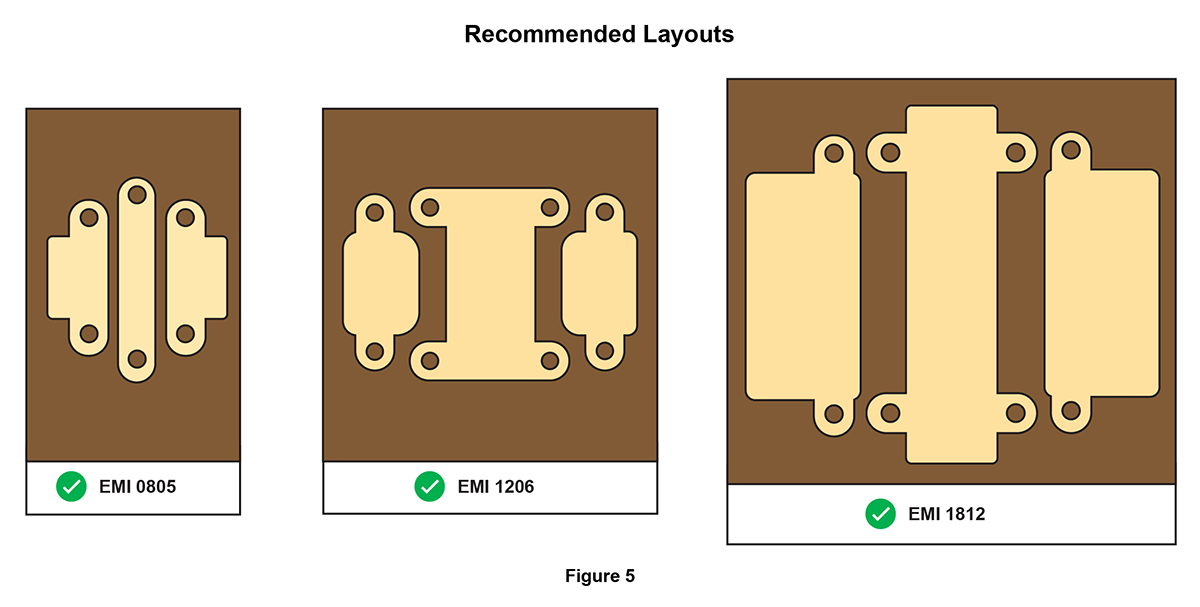
Independent tests confirm that EMI capacitor inductance actually decreases as EMI parts grow larger. The decrease is due to greater distance between like polarity vias, and the additional via pair.
Conclusion
Capacitor land / via patterns play a key role in the realizable performance of bypass capacitors, particularly low inductance EMI capacitors. Attention to: land pattern, via design, and PCB stack-up result in the fewest number of capacitors, and route blocking vias for a given PCB. EMI has seen gains of more than 10:1 achieved from combined use of EMI capacitors and well designed stack-ups, compared to conventional capacitors and poorly thought-outstack-ups.2