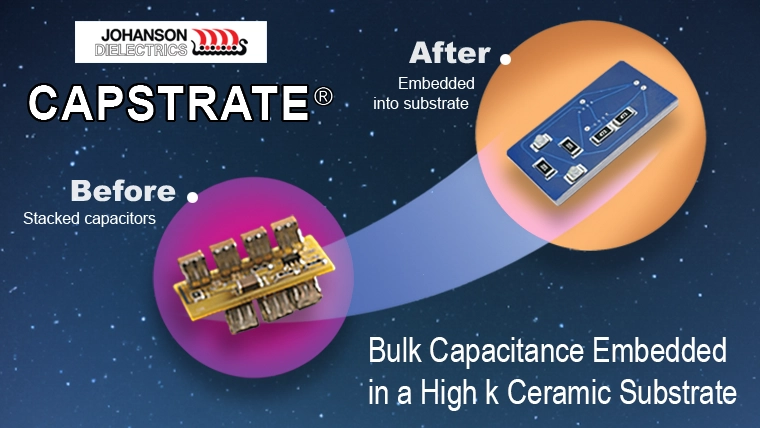
CapStrate® Bulk Capacitance Embedded in a High-k Ceramic Substrate
Design Guide
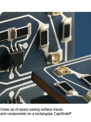
- Customizable to accommodate challenging board layouts "Space Saver"
- Quick turn prototype to high volume production
- Reducing component count and higher reliability
- Unique customer solutions
- One-stop design, manufacturing, and assembly
CapStrate® Selection
Choosing the correct CapStrate® influences the mechanical and electrical function of a design. Johanson Dielectrics offers ceramic substrates for use in application specific environments. It is recommended to choose the right substrate that meets the required electrical requirements and is suitable for the environment the product will operate in.
Johanson Dielectrics offers a variety of materials with a high dielectric constant (K) that can be used within CapStrate® designs. The dielectric constant is directly related to the amount of bulk capacitance that can be realized and allows for compact form factors.
| CapStrate® Material | X7R | NP0 | X8R |
|---|---|---|---|
| Dissipation Factor | <2.5% | <0.15% | <2.5% |
| Dielectric Strength (V/mil) | 200 | 300 | 200 |
| Temperature Coefficient | ±15% | 0 ± 30 ppm/°C | ±15% |
| Temperature Range | -55 °C to +125 °C | -55 °C to +125 °C | -55 °C to +150 °C |
CapStrate® Sizes & Shapes
| Dimension | Minimum | Maximum | Tolerance |
|---|---|---|---|
| Thickness | 0.050” (1.27mm) | 0.215” (5.461mm) | +/- 0.005 (0.127mm) |
| Length | 0.20” (5.08mm) | 2.00”/1.00” (50.8/25.4mm) | +/- 0.005 (0.127mm) |
| Width | 0.20” (5.08mm) | 1.00”/2.00” (25.4/50.8mm) | +/- 0.005 (0.127mm) |
| Temperature Range | -55 °C to +125 °C | -55 °C to +125 °C | -55 °C to +150 °C |
| Dimension | Minimum | Maximum | Tolerance |
|---|---|---|---|
| Thickness | 0.050” (1.27mm) | 0.215” (5.46mm) | +/- 0.005 (0.127mm) |
| Diameter | 0.20” (5.08mm) | 2.00” (50.8mm) | +/- 0.005 (0.127mm) |
Integrating Bulk Capacitance
The advantages of CapStrate® Dielectrics can be fully realized by replacing discrete capacitors with bulk capacitance from the ceramic substrates. The amount of capacitance that can be utilized varies depending on the design dimensions.
Tables 4 and 5 reference the maximum amount of capacitance that can be designed for dimensional, substrate and voltage constraints.
Typical voltage ratings vary from 100 to 1000V, however, engineers are invited to discuss special voltage requirements not listed below.
| NP0 | Length | Width | Thickness | 100V | 250V | 500V | 1000V |
|---|---|---|---|---|---|---|---|
| Maximum Size | 2.00" (50.8mm) | 1.00" (25.4mm) | 0.150" (3.81mm) | 5000nF | 2500nF | 1400nF | 940nF |
| Minimum Size | 0.20" (5.08mm) | 0.20" (5.08mm) | 0.050" (1.27mm) | 30nF | 9nF | 5nF | 2.8nF |
| X7R | Length | Width | Thickness | 100V | 250V | 500V | 1000V |
|---|---|---|---|---|---|---|---|
| Maximum Size | 2.00" (50.8mm) | 1.00" (25.4mm) | 0.150" (3.81mm) | 120000nF | 60000nF | 25000nF | 8000nF |
| Minimum Size | 0.20" (5.08mm) | 0.20" (5.08mm) | 0.050" (1.27mm) | 800nF | 200nF | 70nF | 20nF |
| X8R | Length | Width | Thickness | 100V | 250V | 500V | 1000V |
|---|---|---|---|---|---|---|---|
| Maximum Size | 2.00" (50.8mm) | 1.00" (25.4mm) | 0.150" (3.81mm) | 84000nF | 42000nF | 17500nF | 5600nF |
| Minimum Size | 0.20" (5.08mm) | 0.20" (5.08mm) | 0.050" (1.27mm) | 560nF | 140nF | 49nF | 14nF |
Integrating Bulk Capacitance & Capacitancy Density
- Custom Geometry
- Increased Bulk Capacitance
- High Voltage Capabilities
- Reduction in Size
| NP0 | Diameter | Thickness | 100V | 250V | 500V | 1000V | 1000V |
|---|---|---|---|---|---|---|---|
| Maximum Size | 2.00" (50.8mm) | 0.150” (3.81mm) | 7600nF | 3800nF | 2600nF | 1400nF | 940nF |
| Minimum Size | 0.20" (5.08mm) | 0.050" (1.27mm) | 25nF | 6nF | 3nF | 1.7nF | 2.8nF |
| X7R | Diameter | Thickness | 100V | 250V | 500V | 1000V | 1000V |
|---|---|---|---|---|---|---|---|
| Maximum Size | 2.00" (50.8mm) | 0.150” (3.81mm) | 180000nF | 95000nF | 40000nF | 12000nF | 8000nF |
| Minimum Size | 0.20" (5.08mm) | 0.050" (1.27mm) | 550nF | 140nF | 45nF | 15nF | 20nF |
| X8R | Diameter | Thickness | 100V | 250V | 500V | 1000V | 1000V |
|---|---|---|---|---|---|---|---|
| Maximum Size | 2.00" (50.8mm) | 0.150” (3.81mm) | 126000nF | 66500nF | 28000nF | 8400nF | 5600nF |
| Minimum Size | 0.20" (5.08mm) | 0.050" (1.27mm) | 385nF | 98nF | 31.5nF | 10.5nF | 14nF |
Additional sizes and form factors not listed are possible. Contact Johanson to assess the feasibility of your design. Reference table 6 for the maximum capacitance density that can be used for a given substrate. Capacitance density, below, is presented in nF/(mils)3. This is the maximum amount of capacitance available in a given volume.
| Rectangular | X7R | NP0 | X8R | Circular | X7R | NP0 | X8R |
|---|---|---|---|---|---|---|---|
| 100V | 4.00E-04 | 1.67E-05 | 2.80E-04 | 100V | 3.82E-04 | 1.61E-02 | 1.13E-02 |
| 250V | 2.00E-04 | 8.33E-06 | 1.40E-04 | 250V | 2.02E-04 | 8.10E-03 | 5.67E-03 |
| 500V | 8.33E-05 | 4.67E-06 | 5.83E-05 | 500V | 8.49E-05 | 5.51E-03 | 3.86E-03 |
| 1000V | 2.67E-05 | 3.13E-06 | 1.87E-05 | 1000V | 2.54E-05 | 2.97E-03 | 2.08E-03 |
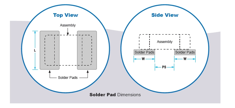
Metallization/Solder Pads
Johanson Dielectrics offers a variety of metallization schemes that are high reliability conductors. These metals can be utilized as conductors, solder pads, or methods of thermal transfer. Designers should select the available metal based on the metallization properties that best suit their design. Careful selection of particular metallizations is dependent on requirements for solderability, temperature resistance, and electrical performance.
| Dielectric | Ag / Pt | Ni / Au | Ag / Ni / Au |
|---|---|---|---|
| X7R | X | X | - |
| X8R | X | X | - |
| NP0 | X | - | X |
| Material Property | Ag / Pt | Ni / Au | Ag / Ni / Au |
|---|---|---|---|
| Recommended Thickness | 14µm | 7-12µ” | Contact Factory |
| Max Solder Temp | 218°C | 260°C | 230°C |
| Metallization | Length (Minimum) | Width (Minimum) | Pad Spacing (Minimum) |
|---|---|---|---|
| Ag/Pt | 0.015" (0.381mm) | 0.010" (0.254mm) | 0.007" (0.178mm) |
| Ni/Au | 0.015" (0.381mm) | 0.010" (0.254mm) | 0.007" (0.178mm) |
| Ag/Ni/Au | 0.015" (0.381mm) | 0.010" (0.254mm) | 0.007" (0.178mm) |
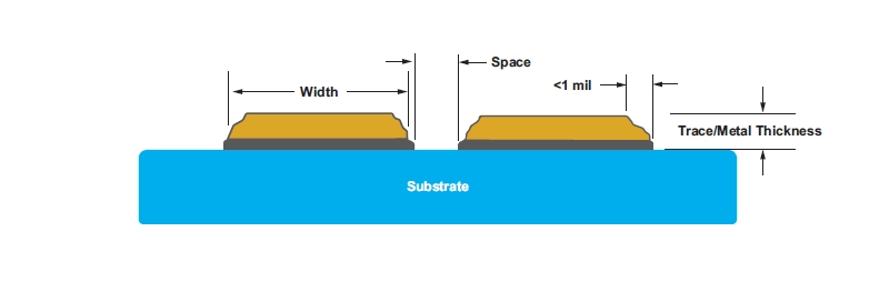
Traces & Tolerances
Vias Definition & Dimensions
Vias are used to connect different layers in the CapStrate® as a means of an electrical or thermal connection. Johanson Dielectrics offers plated through-hole vias for designers to use
| Via Style | Hole Diameter(Minimum) | Hole to Hole(Minimum Spacing) | Via to Edge(Minimum Spacing) | Plated Through-hole |
|---|---|---|---|---|
| Plated Through-hole | 0.028"(0.771mm) | 0.012"(0.305mm) | 0.015"(0.381mm) | 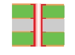 |
"We encourage all designers to submit their drawings or ideas for quick and easy feedback."
Assembly Services
Available in-house
Includes: but is not limited to, soldering resistors, inductors, wires and transistors. One-stop design, manufacturing, and assembly ensures customers receive completed product, without the hassle of developing an assembly stations.

How to Submit Custom CapStrate® Designs
- Follow Johanson’s design guidelinesand standard specifications.
- Provide CAD data in multiple layers.
- Identify “A” side and “B” sidefor double-patterned circuits.
- Provide tolerances and annotation.
- List CapStrate® type, dimensions, and rated voltage.
- Specify metallizations, thickness and tolerances, pads.
- Specify conductor traces, type, spacing, and tolerances.
- List any environmental or electrical testing needed.
- Other inspection or acceptance criteria.
Don't miss the opportunity to work with our outstanding design engineers.
Send us a message for more information. We look forward to assisting you with your unique design requirements.
Johanson Dielectrics has a specialized high-reliability department with extensive in-house testing capabilities. Our testing includes, but is not limited to the following:
Electrical & Mechanical Inspections
- 100% Visual Inspection
- DWV, Voltage Breakdown
- Capacitance, Dissipation Factor
- Resistance & Continuity Testing
- Temperature Voltage Coefficient(TVC)
- Temperature CapacitanceCoefficient (TCC)
Environmental Testing
- Bond Pull Test
- Temperature Cycling
- Resistance to Solder Heat
- Shock and Vibration Testing
Analytical Testing
- SEM Inspection
- Solderability Testing
- Destructive Physical Analysis

Quality Commitments JOHANSON DIELECTRICS
Commitments and Certifications We are committed to making products of the highest quality, performance, and value. Our new design and manufacturing facility employs state of the art equipment and practices. All employees participate in quality awareness and SPC training classes, and our quality system is certified to ISO 9001.

RoHS Standard parts supplied by Johanson Dielectrics, Inc. are fully compliant to the European Union Directives 2002/95/EC, 2011/65/EU, and Annex II (EU) 2015/863 of the European Parliament and of the Council of 31 March 2015 on the Restriction of the use of certain Hazardous Substances in electrical and electronics equipment (RoHS Directives).

REACH Parts (articles) supplied by Johanson Dielectrics meet the requirements for REACH and do not contain any of the SVHC chemicals listed above the levels mandated by the ECHA.